Piezoelectric Capabilities

Please Wait
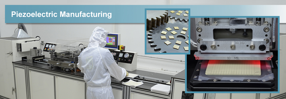
Thorlabs manufactures a broad variety of piezoelectric (PZT) devices including chips, discrete stacks, and amplified actuators. Our integrated in-house manufacturing facility in Shanghai, China allows us to produce precise, reliable piezoelectric devices at an economical price for OEM solutions as well as special applications. Thorlabs' capacity for high-volume production ensures short lead times for large quantity orders.
Our extensive line of PZT products can be used in various fields:
- Semiconductor Technology
- Optoelectronics
- Communications & Integrated Optics
- Biotechnology & Life Science Technology
- Precision Machining
- Medical Technology & Drug Design
- Data Storage Technology
- Nanotechnology
- Nano-Manufacturing & Nano-Automation
- Astronautics
- Image Processing
Click on the tabs above or the pictures below to explore our piezoelectric product line and learn about our capabilities for each step of the manufacturing process.
Click to Enlarge
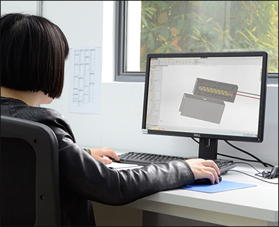
An Engineer Designing a Piezo Actuator
Piezoelectric Design Capabilities
Thorlabs has fabrication and packaging capabilities that enable us to produce a wide range of piezoelectric elements and devices:
- Extensive Expertise in Design and Manufacture of Piezoelectrics
- Partially-Automated Production Line for
- Large-Volume Production
- High Quality and Stabile Performance
- Excellent Accuracy Across Product Lines
- Short Lead Times
- Piezoelectric Chips, Stacks, and Amplified Actuators Available from Stock
Thorlabs manufactures a large range of compact piezoelectric chips, stacks, and actuators that are ideal for many research and industrial applications. These include chips with in-chip and on-stack insulation, discrete stacks fabricated from multiple individual chips bonded together with an epoxy-based binder, and co-fired stacks that are sintered as a single monolithic unit. We offer bimorph benders, piezo devices with integrated strain gauges for closed-loop operation, and multi-axis positioners. Our chips and stacks are available with square, circular, and ring cross sections, and we offer a selection whose displacement is along the lateral direction (shear piezos).
Our team of experts has extensive expertise in the design, manufacture, and development of piezo devices. In addition to the standard items we offer from stock, our manufacturing capabilities allow us to accommodate requests for piezo chips and stacks with customized cross-sections and thicknesses. The capacitance and maximum voltage may also be customized.
Cross sectional dimensions can be varied from 0.7 mm to 85 mm, and our processing equipment can accommodate the manufacture of chips with thicknesses between 0.5 mm and 25 mm. We recommend limiting the thickness of chips fabricated using the in-chip insulation technique to ≤3 mm to protect against cracks developing in the chip during operation; thicknesses less than 3 mm ensure stresses developing at the boundary between the active and insulating region of the chip remain within safe levels.
Multilayer PZT Chip Design Capabilities
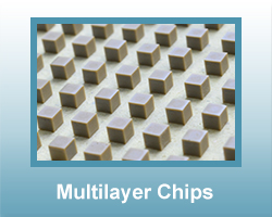
Our team of engineers utilizes a large selection of tools and design capabilities to create an extensive product line of piezo actuators and devices. Thorlabs' manufacturing capabilities give us control over every step of the construction and assembly of these multilayered PZT chips, as shown below.
Click to Enlarge
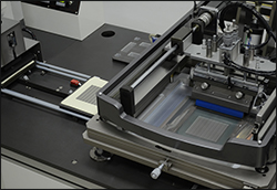
Figure 1: Thorlabs' Screen Printing Machine
Screen Printing of Inner Electrodes & Stacking
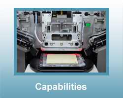
The automatic screen printing equipment (Figure 1) prints the inner electrodes onto every layer of ceramic tape. It uses a silver/palladium paste and a mask that is designed specifically for our stacked PZT devices. Stacking these layers with interconnecting electrodes creates the multilayer PZT block. These machines are capable of large volume production, creating blocks with a high degree of accuracy and efficiency.
Click to Enlarge
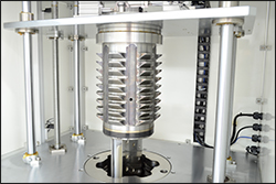
Figure 2: Isobaric Press with Prepped PZT Block
Isostatic Pressing
After screen printing, the PZT block is packaged in a vacuum sealed container and placed in an isostatic press (Figure 2). This press exerts a uniform and specific pressure over the PZT block in order to increase the density of the PZT device. This increase in density leads to improved mechanical properties and workability.
Click to Enlarge
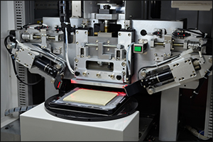
Figure 3: Cutting Machine Slicing a PZT Block
Cutting
Once the PZT block has been properly pressed, it is time to cut the block into individual elements. This is accomplished through the use of a programmable cutting machine (Figure 3). We can cut the block into any size necessary for the final product and according to the pattern of the inner electrodes. This gives our manufacturing capabilities significant customizability options as well as large volume production.
De-Binding and Sintering
Once cut into individual pieces, the binder materials and solvent residues inside the ceramic material, necessary during the manufacturing of the PZT block, need to be cleaned and removed. De-binding (i.e., binder burnout) is accomplished by subjecting the PZTs to a designed heating cycle. This process helps to remove batch-to-batch performance variations and defects, ensuring that our product line functions reliably and reproducibly across the entire manufacturing process.
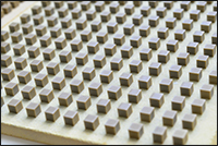
Once binder burnout has been completed, the chips are prepared for sintering. This process is performed at high temperatures that do not melt the ceramic body, but rather fuse the material together. The process continues as crystallites are formed and grow until the optimum device density is achieved.
Click to Enlarge
Figure 4: PZT Chips After Binder Burnout and Sintering
Lapping
To ensure tight dimensional tolerances, we employ high-precision lapping machines to control the thickness of the PZT device in the direction of translation. Our lapping machines (Figure 5) allow us to ensure a 5 µm tolerance on these chips across batches.
Screen Printing Outer Electrodes
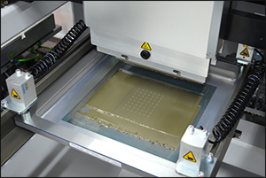
The next step to creating a PZT devices is to create the outer electrodes that will be used for making electrical connections within a system. Our manufacturing process screen prints these electrodes onto each device. To begin, the surfaces of the ceramics are meticulously cleaned to prepare for screen printing. The batch is then placed in a machine designed to print silver metal onto the surfaces of the ceramics (Figure 6) to create the outer electrodes.
Finally, the batch is baked at specific temperatures multiple times and then silver fired to enhance the adhesion between the silver electrodes and the ceramics.
Poling
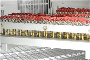
At this point in manufacturing, the ceramic pieces are not yet piezoelectric devices. The sintered PZT chips are isotropic and must undergo poling in order to function as a piezoelectric device. Poling subjects each device to a strong electrical field across the electrodes (Figure 7), which then activates the ceramic's piezoelectric properties.

Click to Enlarge
Figure 5: PR-Hoffman Double-Sided Grinding Machine for Lapping PZT Chips
Click to Enlarge
Figure 6: Screen Printing Electrodes onto PZT Chips
Click to Enlarge
Figure 7: Poling Sintered PZT Chips
Click to Enlarge
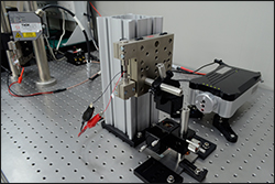
Figure 1: Displacement Testing
Each PZT product manufactured by Thorlabs is subjected to several performance and safety tests before they are shipped to customers. This lab quality management system follows rigorous quality control procedures, which ensure the high quality and performance of each of our piezo devices. Our test capabilities include the following:
- Performance Testing (Stroke, Resonant Frequency, Impedance, etc.)
- Accelerated Lifetime Testing (Assesses the Reliability and Average Lifetime of the Piezo Device)
- Alternating Current Testing (Examines the Insulation Strength)
The method for testing the displacement (stroke) of a piezo device depends on its size. For piezo chips that are 2 mm × 2 mm or larger, we use a high resolution (0.03 µm) micro-epsilon laser displacement sensor. This is a non-contact test, which keeps the chip intact during the testing and ensures highly accurate measured data. For smaller PZT chips (1.5 mm × 1.5 mm and smaller), we employ a Renishaw laser interferometer to measure displacement. This interferometer has a high degree of accuracy (±0.5 ppm) and resolution (0.001 µm). Additionally, it is capable of self-compression, which reduces the environmental impact on the measured data.
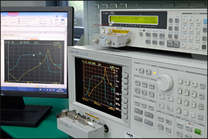
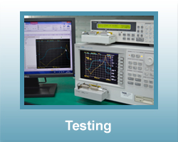
Basic electronic and performance properties, such as impedance, resonant frequency, antiresonant frequency, etc., are investigated using an Agilent Impedance Analyzer.
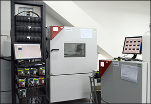
Accelerated lifetime testing assesses the reliability and average lifetime of the PZT device. The reliability and adaptability of the piezo is examined by analyzing its response under high temperature, high humidity, and double voltage conditions. Furthermore, by testing a device’s performance after aging and comparing it to new devices, the reliability and average lifetime of the piezo can be predicted.
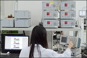
Alternating Current (AC) testing examines the insulation strength of the device by subjecting it to long term alternating voltage and mechanical vibrations.
Click to Enlarge
Figure 4: AC Testing
Click to Enlarge
Figure 3: Accelerated Lifetime Testing
Click to Enlarge
Figure 2: Basic Electronic And Performance Testing
Click to Enlarge
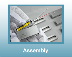
Assembling a Thorlabs' Amplified PZT Actuator
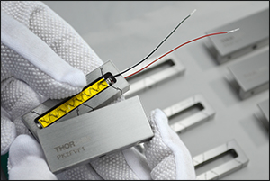
Thorlabs’ Discrete Piezoelectric Stacks are assembled from our individual PZT chips. To assemble a stack, multiple piezoelectric chips are stacked face-to-face and bonded with epoxy and glass beads. Using multiple chips in tandem allows these stacks to achieve free stroke displacements that are significantly larger than their single chip counterparts. The stacks maintain the sub-millisecond response times and low drive voltage ranges of the chips. Each chip is, itself, insulated with a ceramic layer on four sides, resulting in better protection against moisture than common epoxy-coated designs. The remaining two sides contain the screen-printed silver electrodes for electrical connections. Since each ship within the stack undergoes our precision grinding process, the height of the stack can be maintained to an accuracy of ±0.1 mm. Our stacks also come with pre-attached, 75 mm long wires and are wrapped in Kapton tape for additional electrical insulation.
Our Amplified PZT Actuators incorporate our discrete PZT stack within a flexure mount. This combination results in a lever-amplified free stroke displacement, providing a significantly larger displacement than a discrete stack itself. These amplified actuators maintain the same sub-millisecond response times and low drive voltages as our chips and stacks. Because the displacement of these actuators is created by a PZT stack in a flexure mount, it does not suffer from backlash.
| Posted Comments: | |
jiayu wang
(posted 2024-05-14 16:54:06.943) 定制/购买压电陶瓷器件。位移分辨率要求在2-10nm左右
定制/购买压电陶瓷驱动,要求有方形波,三角波,正弦波
单位:中北大学 cdolbashian
(posted 2024-05-24 10:45:42.0) Thank you for contacting Thorlabs. We will reach out to you directly to discuss the possibility of offering this. For future custom requests, please feel free to reach out to your local tech support team (in your case: techsupport-cn@thorlabs.com). Xie Caijin
(posted 2019-10-12 19:36:08.897) Do you offer piezoelectric customization service? We want to customize piezoelectirc. llamb
(posted 2019-10-12 01:25:22.0) Thank you for contacting Thorlabs. Yes, we do offer piezoelectric customization services. You can reach out to your local Thorlabs Technical Support team for customization inquiries (techsupport-cn@thorlabs.com). For this particular case, we will reach out to you directly to discuss your application. jennette.manalo
(posted 2016-05-21 03:21:30.627) Do you sell the screen printing machine for PZT? If yes, kindly provide details such as specifications, price, etc. besembeson
(posted 2016-05-25 10:09:55.0) Response from Bweh at Thorlabs USA: We do not provide this machine at this time. I will contact you with a recommendation. |
 Products Home
 Piezoelectric Manufacturing