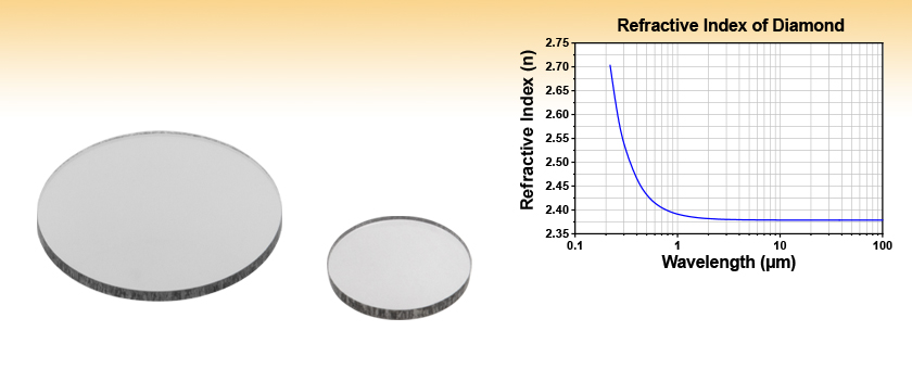
Polycrystalline CVD Diamond Windows

- Diamonds Grown by Chemical Vapor Deposition
- Broad Transmission Spectrum from 220 nm to >50 µm
- Available with 5.0 mm or 10.0 mm Diameters
WGM0505
Ø5.0 mm, 0.5 mm Thick
Polycrystalline CVD Window
WGM1005
Ø10.0 mm, 0.5 mm Thick
Polycrystalline CVD Window

Please Wait

Click to Enlarge
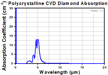
Absorption Plot
| Flat Window Selection Guide | |
|---|---|
| Wavelength Range | Substrate Material |
| 180 nm - 8.0 μm | Calcium Fluoride (CaF2) |
| 185 nm - 2.1 μm | UV Fused Silica |
| 200 nm - 5.0 μm | Sapphire |
| 200 nm - 6.0 μm | Magnesium Fluoride (MgF2) |
| 220 nm to >50 µm | CVD Diamond Windows |
| 230 nm - 1.1 µm | UV Fused Silica, Textured Antireflective Surface |
| 250 nm - 1.6 µm | UV Fused Silica, for 45° AOI |
| 250 nm - 26 µm | Potassium Bromide (KBr) |
| 300 nm - 3 µm | Infrasil® |
| 350 nm - 2.0 μm | N-BK7 |
| 600 nm - 16 µm | Zinc Selenide (ZnSe) |
| 1 - 1.7 µm | Infrasil®, Textured Antireflective Surface |
| 1.2 - 8.0 μm | Silicon (Si) |
| 1.9 - 16 μm | Germanium (Ge) |
| 2 - 5 μm | Barium Fluoride (BaF2) |
| V-Coated Laser Windows | |
Features
- 5.0 mm or 10.0 mm Diameter
- 0.5 mm Thickness
- Polycrystalline Diamonds Grown by Chemical Vapor Deposition (CVD)
- Broad Transmission Spectrum from 220 nm to >50 µm
- High Thermal Conductivity
- >2200 Wm-1K-1 at 300 K
- >1600 Wm-1K-1 at 425 K
These Polycrystalline CVD Diamond Windows are ideal for applications in demanding optical systems. Diamond boasts a broad transmission spectrum (220 nm to >50 µm), as well as a high level of thermal conductivity (>2200 Wm-1K-1 at 300 K, and >1600 Wm-1K-1 at 425 K). The low absorption of these diamond windows allows high power laser light to be transmitted without causing damage to the window itself. Diamond may also be suited for medical applications due to its biocompatibility, and its broad transmission spectrum increases efficiency when used within spectroscopy setups.
For high-vacuum applications, Thorlabs offers our Ø10 mm CVD diamond window integrated into a Ø2.75" (DN40) CF Flange; see the full web presentation for details.
Thorlabs also offers precision windows fabricated from other substrates for use in a large variety of laser and industrial applications. For our complete selection, see the Flat Window Selection Guide table to the right. We also offer laser windows, which have AR coatings centered around commonly used laser wavelengths, and Brewster windows, which are designed to eliminate p-polarized reflected light.
| Item # | WGM0505 | WGM1005 |
|---|---|---|
| Diameter | 5.0 mm | 10.0 mm |
| Diameter Tolerance | ±0.1 mm | |
| Thickness | 0.5 mm | |
| Thickness Tolerance | ±0.05 mm | |
| Flatness | Three Fringes at 632.8 nm | Five Fringes at 632.8 nm |
| Laser Kerf | ≤3° ± 2° | |
| Egde Features | <0.2 mm | |
| Parallelism | <0.4 µm/mm | |
| Roughness (over 1 mm2) | <15 nm | |
| Refractive Index | 2.376 (at 10.6 µm), 2.386 (at 1550 nm), 2.392 (at 1064 nm) | |
| Young's Modulus | 1050 GPa | |
| Fracture Stress | 400 MPa | |
| Hardness | 81 ± 18 GPa | |
| Thermal Expansion Coefficient | 1.0 ppmK-1 (at 300 K), 4.4 ppmK-1 (at 1000 K) | |
| Thermal Conductivity | >2200 Wm-1K-1 (at 300 K), >1600 Wm-1K-1 (at 425 K) | |
| Substrate | CVD Diamond | |
| Absorption Coefficient | <0.07 cm-1 (10.6 µm), 0.12 cm-1 (at 1064 nm) | |

| Posted Comments: | |
Marzuqa Ahmed
(posted 2024-02-01 12:24:57.717) Hello, I would like to know the transmission data for this window as well as the wavelength range.
Please let me know.
Best,
Marzuqa cdolbashian
(posted 2024-02-02 09:32:16.0) Thank you for reaching out to us with this inquiry. This type of diamond has nominally a broadband transmission up to 100um and beyond, though we only really advertise it for up to 25um. Within this range the absorption of the material is relatively low (as you can see in the absorption coefficient graph) and most of the reduction in transmission comes from Fresnel reflections at each air-glass interface. Typical transmission for the low absorption coefficient regions (excluding the 2.5-7.5um region where large absorption occurs) will be approximately 70%. I have contacted you directly to discuss your particular wavelengths of interest. Gary Cook
(posted 2023-08-30 15:38:18.957) the absorption spectrum you show for your diamond windows appears to be incorrect: https://www.thorlabs.com/newgrouppage9.cfm?objectgroup_id=15962&pn=WGM1005
The absorption features you show should occur between 2 microns and 5 microns, and not between 10 microns and 15 microns as you show. Can you double check your data? cdolbashian
(posted 2023-09-11 11:58:10.0) Thank you for reaching out to us with this observation. Looking into various sources on the web, I tend to agree with you here. We will be reviewing this internally, and likely will be updating these graphs. user
(posted 2023-08-30 11:41:49.903) Are you sure the absorption listed is correct? Diamond should not be absorbing at 10um. cdolbashian
(posted 2023-09-11 11:58:12.0) Thank you for voicing this concern. Upon further review, we tend to agree with you on this point. We will be updating this in the near future. |
| Window Selection Guide (Table Sorted by Wavelength) | |||||
|---|---|---|---|---|---|
| Substrate and Window Type | Wavelength Range | Available AR Coatings | Reflectance over AR Coating Rangea | Transmission Data | Reflectance Data |
| Calcium Fluoride (CaF2): Flat or Wedged |
180 nm - 8.0 μm | Uncoated | - | Raw Data |
- |
| -D Coating, 1.65 - 3.0 µm | Ravg < 1.0%; Rabs < 2.0% at 0° AOI | Raw Data |
Raw Data |
||
| UV Fused Silica: Flat, Wedged, V-Coated Flat, or V-Coated Wedged |
185 nm - 2.1 μm | Uncoated (Flat or Wedged) |
- | Raw Data |
- |
| -UV Coating, 245 - 400 nm (Flat or Wedged) |
Ravg < 0.5% at 0° AOI | - | Raw Data |
||
| -C3 Coating, 261 - 266 nm (V-Coated) |
Ravg < 0.5% at 0° AOI | - | Raw Data |
||
| -C6 Coating, 350 - 450 nm (V-Coated) |
Ravg < 0.5% at 0° AOI | - | Raw Data |
||
| -A Coating, 350 - 700 nm (Flat or Wedged) |
Ravg < 0.5% at 0° AOI | - | Raw Data |
||
| -B Coating, 650 - 1050 nm (Flat or Wedged) |
Ravg < 0.5% at 0° AOI | - | Raw Data |
||
| -C Coating, 1050 - 1700 nm (Flat or Wedged) |
Ravg < 0.5% at 0° AOI | - | Raw Data |
||
| Sapphire: Flat or Wedged |
200 nm - 5.0 μm | Uncoated | - | Raw Data |
- |
| -D Coating, 1.65 - 3.0 µm | Ravg < 1.0% at 0° AOI | Raw Data |
Raw Data |
||
| -E1 Coating, 2.0 - 5.0 µm | Ravg < 1.50%, Rabs < 3.0% (per Surface, 2.0 - 5.0 µm); Ravg < 1.75% (per Surface, 2.0 - 4.0 µm) at 0° AOI |
Raw Data |
Raw Data |
||
| Magnesium Fluoride (MgF2): Flat or Wedged |
200 nm - 6.0 μm | Uncoated | - | Raw Data |
- |
| Barium Fluoride (BaF2): Flat or Wedged |
200 nm - 11 µm | Uncoated (Wedged Only) |
- | Raw Data |
- |
| -E1 Coating, 2 - 5 µm | Ravg < 1.25%; Rabs < 2.5% at 0° AOI | Raw Data |
Raw Data |
||
| UV Fused Silica, for 45° AOI: Flat or Wedged |
250 nm - 1.6 µm | Coating for 250 nm - 450 nm |
Ravg < 1.0% at 45° AOI | Raw Data |
|
| Coating for 350 nm - 1100 nm |
Ravg < 2.0% at 45° AOI | Raw Data |
|||
| Coating for 400 nm - 700 nm |
Ravg < 1.0% at 45° AOI | Raw Data |
|||
| Coating for 600 nm - 1700 nm |
Ravg < 1.5% at 45° AOI | Raw Data |
|||
| Coating for 700 nm - 1100 nm |
Ravg < 1.0% at 45° AOI | Raw Data |
|||
| Coating for 1200 nm - 1600 nm |
Ravg < 1.0% at 45° AOI | Raw Data |
|||
| Potassium Bromide (KBr): Flat |
250 nm - 26 µm | Uncoated | - | - | |
| Infrasil®: Flat |
300 nm - 3 µm | Uncoated | - | Raw Data |
- |
| N-BK7: Flat, Wedged, V-Coated Flat, or V-Coated Wedged |
350 nm - 2.0 μm | Uncoated (Flat or Wedged) |
- | Raw Data |
- |
| -A Coating, 350 - 700 nm (Flat or Wedged) |
Ravg < 0.5% at 0° AOI | - | Raw Data |
||
| -C7 Coating, 400 - 700 nm (V-Coated) |
Ravg < 0.5% at 0° AOI | - | Raw Data |
||
| -C10 Coating, 523 - 532 nm (V-Coated) |
Ravg < 0.5% at 0° AOI | - | Raw Data |
||
| -C11 Coating, 610 - 860 nm (V-Coated) |
Ravg < 0.5% at 0° AOI | - | Raw Data |
||
| -B Coating, 650 - 1050 nm (Flat or Wedged) |
Ravg < 0.5% at 0° AOI | - | Raw Data |
||
| -C13 Coating, 700 - 1100 nm (V-Coated) |
Ravg < 0.5% at 0° AOI | - | Raw Data |
||
| C14 Coating, 1047 - 1064 nm (V-Coated) |
Ravg < 0.5% at 0° AOI | - | Raw Data |
||
| -C15 Coating, 523 - 532 nm & 1047 - 1064 nm (V-Coated) |
Ravg < 0.5% at 0° AOI | - | Raw Data |
||
| -C Coating, 1050 - 1700 nm (Flat or Wedged) |
Ravg < 0.5% at 0° AOI | - | Raw Data |
||
| Zinc Selenide (ZnSe): Flat or Wedged |
600 nm - 16 µm | Uncoated | - | Raw Data |
- |
| -D Coating, 1.65 - 3.0 µm | Ravg < 1.0%; Rabs < 2.0% at 0° AOI | Raw Data |
Raw Data |
||
| -E4 Coating, 2 - 13 µm (Only Flat) |
Ravg < 3.5%; Rabs < 6% at 0° AOI | Raw Data |
Raw Data |
||
| -E2 Coating, 4.5 - 7.5 µm (Only Flat) |
Ravg < 1.0%; Rabs < 2.0% at 0° AOI | Raw Data |
Raw Data |
||
| -E3 Coating, 7 - 12 µm (Only Wedged) |
Ravg < 1.0%; Rabs < 2.0% at 0° AOI | Raw Data |
Raw Data |
||
| -G Coating, 7 - 12 µm (Only Flat) |
Ravg < 1% at 0° AOI | Raw Data |
Raw Data |
||
| Silicon (Si): Flat or Wedged |
1.2 - 8.0 μm | Uncoated | - | Raw Data |
- |
| -E1 Coating, 2 - 5 µm (Only Wedged) |
Ravg < 1.25%; Rabs < 2.5% at 0° AOI | Raw Data |
Raw Data |
||
| -E Coating, 3 - 5 µm (Only Flat) |
Ravg < 2% at 0° AOI | Raw Data |
Raw Data |
||
| Germanium (Ge): Flat or Wedged |
1.9 - 16 μm | Uncoated, 2.0 - 16 μm | - | Raw Data |
- |
| -C9 Coating, 1.9 - 6 µm (Only Flat) |
Ravg < 2% at 0° AOI | Raw Data |
Raw Data |
||
| -E3 Coating, 7 - 12 µm | Ravg < 1.0%; Rabs < 2.0% at 0° AOI | Raw Data |
Raw Data |
||
 Products Home


 Polycrystalline CVD Diamond Windows